
Author Affiliations
Abstract
1 DTU Electro, Department of Electrical and Photonics Engineering, Technical University of Denmark, DK-2800 Kgs. Lyngby, Denmark
2 Jiaxing Key Laboratory of Photonic Sensing & Intelligent Imaging, Jiaxing 314000, China
3 Intelligent Optics & Photonics Research Center, Jiaxing Research Institute Zhejiang University, Jiaxing 314000, China
An optical phased array (OPA), the most promising non-mechanical beam steering technique, has great potential for solid-state light detection and ranging systems, holographic imaging, and free-space optical communications. A high quality beam with low sidelobes is crucial for long-distance free-space transmission and detection. However, most previously reported OPAs suffer from high sidelobe levels, and few efforts are devoted to reducing sidelobe levels in both azimuthal () and polar () directions. To solve this issue, we propose a Y-splitter-assisted cascaded coupling scheme to realize Gaussian power distribution in the azimuthal direction, which overcomes the bottleneck in the conventional cascaded coupling scheme and significantly increases the sidelobe suppression ratio (SLSR) in the direction from 20 to 66 dB in theory for a 120-channel OPA. Moreover, we designed an apodized grating emitter to realize Gaussian power distribution in the polar direction to increase the SLSR. Based on both designs, we experimentally demonstrated a 120-channel OPA with dual-Gaussian power distribution in both and directions. The SLSRs in and directions are measured to be and , respectively. Furthermore, we steer the beam to the maximum field of view of with a periodic pitch (3.1 μm). The maximum total power consumption is only 0.332 W with a thermo-optic efficiency of .
Photonics Research
2023, 11(4): 659

Author Affiliations
Abstract
Silicon photonics integrated with graphene provides a promising solution to realize integrated photodetectors operating at the communication window thanks to graphene’s ultrafast response and compatibility with CMOS fabrication process. However, current hybrid graphene/silicon photodetectors suffer from low responsivity due to the weak light-graphene interaction. Plasmonic structures have been explored to enhance the responsivity, but the intrinsic metallic Ohmic absorption of the plasmonic mode limits its performance. In this work, by combining the silicon slot and the plasmonic slot waveguide, we demonstrate a novel double slot structure supporting high-performance photodetection, taking advantages of both silicon photonics and plasmonics. With the optimized structural parameters, the double slot structure significantly promotes graphene absorption while maintaining low metallic absorption within the double slot waveguide. Based on the double slot structure, the demonstrated photodetector holds a high responsivity of 603.92 mA/W and a large bandwidth of 78 GHz. The high-performance photodetector provides a competitive solution for the silicon photodetector. Moreover, the double slot structure could be beneficial to a broader range of hybrid two-dimensional material/silicon devices to achieve stronger light-matter interaction with lower metallic absorption.Silicon photonics integrated with graphene provides a promising solution to realize integrated photodetectors operating at the communication window thanks to graphene’s ultrafast response and compatibility with CMOS fabrication process. However, current hybrid graphene/silicon photodetectors suffer from low responsivity due to the weak light-graphene interaction. Plasmonic structures have been explored to enhance the responsivity, but the intrinsic metallic Ohmic absorption of the plasmonic mode limits its performance. In this work, by combining the silicon slot and the plasmonic slot waveguide, we demonstrate a novel double slot structure supporting high-performance photodetection, taking advantages of both silicon photonics and plasmonics. With the optimized structural parameters, the double slot structure significantly promotes graphene absorption while maintaining low metallic absorption within the double slot waveguide. Based on the double slot structure, the demonstrated photodetector holds a high responsivity of 603.92 mA/W and a large bandwidth of 78 GHz. The high-performance photodetector provides a competitive solution for the silicon photodetector. Moreover, the double slot structure could be beneficial to a broader range of hybrid two-dimensional material/silicon devices to achieve stronger light-matter interaction with lower metallic absorption.
graphene silicon photonics photodetectors Opto-Electronic Advances
2022, 5(12): 210159
Center for Silicon Photonics for Optical Communication, Technical University of Denmark, 2800 Kgs. Lyngby, Denmark
Frontiers of Optoelectronics
2022, 15(1): s12200

Author Affiliations
Abstract
1 Wuhan National Laboratory for Optoelectronics, School of Optical and Electronic Information, Huazhong University of Science and Technology, Wuhan 430074, China
2 Department of Photonics Engineering, Technical University of Denmark, 2800 Lyngby, Denmark
3 SiPhotonIC ApS, 2830 Virum, Denmark
4 e-mail: hailongzhou@hust.edu.cn
Encircling an exceptional point (EP) in a parity-time (PT) symmetric system has shown great potential for chiral optical devices, such as chiral mode switching for symmetric and antisymmetric modes. However, to our best knowledge, chiral switching for polarization states has never been reported, although chiral polarization manipulation has significant applications in imaging, sensing, communication, etc. Here, inspired by the anti-PT symmetry, we demonstrate, for the first time to our best knowledge, an on-chip chiral polarizer by constructing a polarization-coupled anti-PT symmetric system. The transmission axes of the chiral polarizer are different for forward and backward propagation. A polarization extinction ratio of over 10 dB is achieved for both propagating directions. Moreover, a telecommunication experiment is performed to demonstrate the potential applications in polarization encoding signals. It provides a novel functionality for encircling-an-EP parametric evolution and offers a new approach for on-chip chiral polarization manipulation.
Photonics Research
2022, 10(1): 01000076

Author Affiliations
Abstract
1 Wuhan National Laboratory for Optoelectronics and School of Optical and Electrical Information, Huazhong University of Science and Technology, Wuhan 430074, China
2 Department of Photonics Engineering, Technical University of Denmark, Building 343, 2800 Kgs. Lyngby, Denmark
The hybrid multiplexing technique reactivates optical interconnect as it offers multiple dimensions to dramatically enhance the data capacity of a single wavelength carrier. A straightforward method to realize hybrid multiplexing is to perform polarization multiplexing for mode-multiplexed signals, by utilizing a mode-transparent polarization beam splitter (MTPBS) which can process multiple modes simultaneously. However, present PBSs mainly work in the single-mode regime, and it is not easy to redesign the conventional PBS to accommodate multiple modes, due to the severe mode dispersion. Here, a novel MTPBS, which can tackle a group of modes simultaneously, is proposed and demonstrated. As a demonstration, the MTPBS supporting a total channel number of 13 is experimentally achieved, with low insertion loss and low modal/polarization cross talk. This work provides a new insight to realize hybrid multiplexing and represents a solution for high-density and large-capacity photonic integration.
Photonics Research
2020, 8(6): 06000978
1 哈尔滨师范大学计算机科学与信息工程学院, 黑龙江 哈尔滨 150052
2 黑龙江工程学院电气与信息工程学院, 黑龙江 哈尔滨 150050
3 哈尔滨工业大学可调谐激光技术国家级重点实验室, 黑龙江 哈尔滨 150080
为了充分利用相位调制信号中的多普勒频移信息,将相位调制信号的直流和拍频分量中的鉴频参量相结合,构造出一个新的鉴频参量。在理论和实验上,通过依次比较表明新鉴频参量继承了相位调制拍频信号振幅多普勒频移测量方法的特点和优势,相比之下,测量动态范围约提高1倍,测量精度约提高6倍。为了有效利用闲置的回波信号光功率,提出了基于新鉴频参量的双边缘相位调制多普勒频移测量方法,在理论上证明其可将测量灵敏度提高1倍。
遥感 激光雷达 多普勒频移 相位调制 拍频 法布里-珀罗干涉仪

Author Affiliations
Abstract
1 National Laboratory for Optoelectronics, School of Optical and Electronic Information, Huazhong University of Science and Technology, Wuhan 430074, China
2 Department of Photonics Engineering, Technical University of Denmark, 2800 Kgs. Lyngby, Denmark
Tunable optical delay lines are one of the key building blocks in optical communication and microwave systems. In this work, tunable optical delay lines based on integrated grating-assisted contradirectional couplers are proposed and experimentally demonstrated. The device performance is comprehensively improved in terms of parameter optimization, apodization analysis, and electrode design. Tunable group delay lines of 50 ps at different wavelengths within the bandwidth of 12 nm are realized with a grating length of 1.8 mm. Under thermal tuning mode, the actual delay tuning range is around 20 ps at 7.2 V voltage. At last, a new scheme adopting an ultra-compact reflector for doubling group delay is proposed and verified, achieving a large group delay line of 400 ps and a large dispersion value up to 5.5×10⁶ ps/(nm·km) within bandwidth of 12 nm. Under thermal tuning mode, the actual delay tuning range is around 100 ps at 8 V voltage.
Integrated optics devices Wavelength filtering devices Optical buffers Photonics Research
2018, 6(9): 09000880
Author Affiliations
Abstract
1 College of Advanced Interdisciplinary Studies, National University of Defense Technology, Changsha 410073, China
2 Department of Photonics Engineering, Technical University of Denmark, Kgs. Lyngby 2800, Denmark
3 Center of Material Science, College of Liberal Arts and Sciences, National University of Defense Technology, Changsha 410073, China
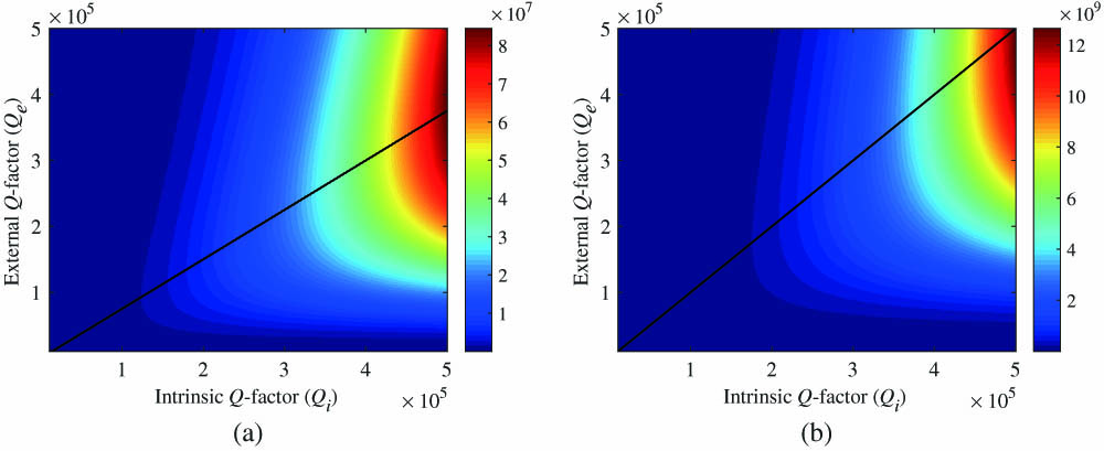
To achieve photon-pair generation scaling, we optimize the quality factor of microring resonators for efficient continuous-wave-pumped spontaneous four-wave mixing. Numerical studies indicate that a high intrinsic quality factor makes high pair rate and pair brightness possible, in which the maximums take place under overcoupling and critical-coupling conditions, respectively. We fabricate six all-pass-type microring resonator samples on a silicon-on-insulator chip involving gap width as the only degree of freedom. The signal count rate, pair brightness, and coincidence rate of all the samples are characterized, which are then compared with the modified simulations by taking the detector saturation and nonlinear loss into account. Being experimentally validated for the first time to the best of our knowledge, this work explicitly demonstrates that reducing the round-trip loss in a ring cavity and designing the corresponding optimized gap width are more effective to generate high-rate or high-brightness photon pairs than the conventional strategy of simply increasing the quality factor.
Nonlinear optics, four-wave mixing Quantum optics Nonlinear optics, devices Photonics Research
2018, 6(6): 06000587
1 Wuhan National Laboratory for Optoelectronics (WNLO), Huazhong University of Science and Technology, Wuhan 430074, China
2 Department of Photonics Engineering, Technical University of Denmark, 2800 Kgs. Lyngby, Denmark
3 State Key Laboratory of Optoelectronic Materials and Technologies, School of Physics and Engineering, Sun Yatsen University,Guangzhou 510275, China
4 Centre for Quantum Photonics, H. H. Wills Physics Laboratory, Department of Electrical and Electronic Engineering,University of Bristol, Bristol BS8 1UB, UK
In this paper, we proposed and experimentally demonstrated a route-asymmetrical light transmission scheme based on the thermal radiative effect, which means that forward and backward propagations of an optical device have different transmittances provided they are not present simultaneously. Employing a fiber-chipfiber optomechanical system, our scheme has successfully achieved a broad operation bandwidth of at least 24 nm and an ultra-high route-asymmetrical transmission ratio (RATR) up to 63 dB. The route-asymmetrical device has been demonstrated effectively with not only the continuous- wave (CW) light but also 10 Gbit/s on-off-keying (OOK) digital signals. Above mentioned unique features can be mostly attributed to the significant characteristics of the thermal radiative effect, which could cause a fiber displacement up to tens of microns. The powerful and significant thermal radiative effect opens up a new opportunity and method for route-asymmetrical light transmission. Moreover, this research may have important applications in all-optical systems, such as the optical limiters and ultra-low loss switches.
route-asymmetrical light transmission route-asymmetrical light transmission thermal radiative effect thermal radiative effect optomechanical system optomechanical system route-asymmetrical transmission ratio (RATR) route-asymmetrical transmission ratio (RATR) Frontiers of Optoelectronics
2016, 9(3): 489
1 Department of Photonics Engineering, Technical University of Denmark, 2800 Kgs. Lyngby, Denmark
2 FOTON Laboratory, CNRS UMR 6082, ENSSAT, University of Rennes 1, F-22305 Lannion, France
3 Wuhan National Laboratory for Optoelectronics, Huazhong University of Science and Technology, Wuhan 430074, China
Wavelength conversion based on degenerate four-wave mixing (FWM) was demonstrated and compared between silicon nanowire and microring resonator (MRR). 15 dB enhancement of conversion efficiency (CE) with relatively low input pump power (5 mW) was achieved experimentally in an MRR. The impacts of bus waveguide length and propagation loss were theoretically analyzed under the effect of nonlinear loss.
wavelength conversion wavelength conversion four-wave mixing(FWM) four-wave mixing(FWM) silicon nanowaire silicon nanowaire microring resonator (MRR) microring resonator (MRR) Frontiers of Optoelectronics
2016, 9(3): 390


